NodeMCU
ESP8266 ESP8266 dev board on an ESP-12 module with 4 MB of flash, FLASH and RST buttons and micro-USB. Wi-Fi only, no Bluetooth.
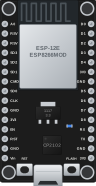
Variants and how to tell them apart
- Flash
- 4 MB
Narrow board, fits a breadboard with a free row on each side.
- Flash
- 4 MB
Wider board, the USB chip is marked CH340G.
Specifications
Figures for NodeMCU v2 (DevKit v1.0, Amica, CP2102).
- Chip
- ESP8266EX
- Module
- ESP-12E (4 MB flash)
- Processor
- 1 core, Tensilica L106, 160 MHz
- RAM
- about 50 KB free with Wi-Fi
- Flash
- 4 MB
- Wi-Fi
- Wi-Fi 4, 2.4 GHz
- USB
- micro-USB
- Logic level
- 3.3 V
- Free GPIO
- 12
- Analog inputs
- 1
- Size
- 25.4 × 48.3 mm
Sources
Checked against these documents on October 15, 2026.
Common problems
The board does not start after wiring D3, D4 or D8
These pins set the boot mode. At power on GPIO15 (D8) must be low, GPIO2 (D4) and GPIO0 (D3) high. Move the wire to another pin.
A 5 V sensor on a GPIO pin
The logic is 3.3 V, the datasheet limit for an input is 3.6 V. Use a level shifter for 5 V signals.
It does not wake up from deep sleep
Connect D0 (GPIO16) to RST: the timer wakes the chip through this wire.
Projects for this board
Tasmota for ESP8266
Local smart home firmware for ESP8266 boards: sensors, relays, rules and a web page, with MQTT and no cloud.No solderingAbout 15 min 2 boardsJust the boardCan be built in an evening
WLED
Web page and phone control for WS2812B LED strips on an ESP8266: effects, palettes, presets and timers.SolderingAbout 30 min2 boardsBesides the board: WS2812B LED strip and 1 moreCan be built in an eveningPinout
NodeMCU v2 (DevKit v1.0, Amica, CP2102), top view.
Left row (J1)
| Pin | Chip pin | What it does |
|---|---|---|
| A0 | TOUT | analog input only, voltage divider on the board |
| RSV | ||
| RSV | Not connected not connected | |
| SD3 | GPIO10 | taken by flash, leave it free |
| SD2 | GPIO9 | taken by flash, leave it free |
| SD1 | GPIO8 | taken by flash, leave it free |
| CMD | GPIO11 | taken by flash, leave it free |
| SD0 | GPIO7 | taken by flash, leave it free |
| CLK | GPIO6 | taken by flash, leave it free |
| GND | Ground | |
| 3V3 | Power, 3.3 V power input, power output | |
| EN | Reset or enable pull-up on the board | |
| RST | Reset or enable button on the board, pull-up on the board | |
| GND | Ground | |
| Vin | Power, 5 V power input, power output |
Right row (J2)
| Pin | Chip pin | What it does |
|---|---|---|
| D0 | GPIO16 | LED on the board |
| D1 | GPIO5 | I2C SCL |
| D2 | GPIO4 | I2C SDA |
| D3 | GPIO0 | affects boot, button on the board |
| D4 | GPIO2 | affects boot, LED on the board |
| 3V3 | Power, 3.3 V power input, power output | |
| GND | Ground | |
| D5 | GPIO14 | HSPI SCK |
| D6 | GPIO12 | HSPI MISO |
| D7 | GPIO13 | HSPI MOSI, UART0 RX (Serial.swap) |
| D8 | GPIO15 | HSPI CS (SS), UART0 TX (Serial.swap) affects boot |
| RX | GPIO3 | UART0 RX |
| TX | GPIO1 | UART0 TX sends a signal at boot |
| GND | Ground | |
| 3V3 | Power, 3.3 V power input, power output |
Have a project for NodeMCU? Publish it, and it shows up on this page.